Semiconductor Patent Drawings
Semiconductor figures live and die by the cross-section — and the cross-section lives and dies by hatching. Every material gets its own pattern, every layer gets its numeral, and the process figures must agree with the structure figures.
- Distinct hatching per material
- Layered cross-sections
- Process flow figures
- Structure–process numeral sync
The 30-second answer
- Structure claims → layered cross-sections with a different hatching pattern for every material — adjacent layers must never share a pattern (37 CFR 1.84(h)(3) governs sectional hatching).
- Process claims → flowcharts, ideally paired with cross-sections at each stage that reuse the structure figures’ layer numerals.
- Layer thicknesses may be exaggerated for legibility — say "not to scale" in the brief description — and generate, number, and check the set in PatentFig AI before filing.
Semiconductor figure examples
Each example is a fictional invention. Open one to pre-fill the generator with the prompt.
Which figures support which claims
Semiconductor claims split into structure, process, and package — each with its canonical figure.
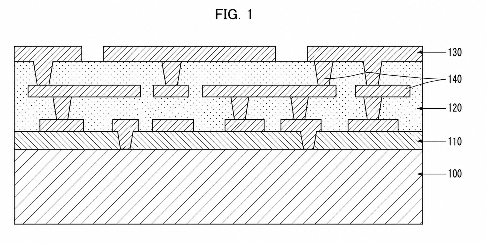
Structure claims → layered cross-sections
The device stack cut vertically: substrate, wells, gate stack, spacers, contacts, metallization — every material with its own hatching pattern and every layer numbered.
Process claims → flowcharts
Deposit, pattern, etch, implant, anneal as numbered steps mirroring the claim — the backbone figure for a method-of-manufacture claim.
Process claims → stage cross-sections
A FIG. 2A–2E series showing the stack after each major step, reusing the same layer numerals so the flowchart, the stages, and the final structure all agree.
Package claims → package cross-sections
Die, solder bumps, interposer, substrate, mold compound, and balls in section — distinct hatching again, since dissimilar materials meet everywhere.
Circuit-level claims → schematics and block diagrams
When claims reach the circuit, standard schematic symbols with numbered components — a different figure type from the physical stack.
Semiconductor drawing mistakes that cost office actions
The failure patterns specific to stack and process figures.
Adjacent layers with identical hatching
If the oxide and the nitride hatch the same way, the boundary disappears and the disclosure with it. Assign every material a visibly distinct pattern and keep it constant across all figures.
Distorted layer scale with no disclaimer
A 2 nm gate oxide drawn at visible thickness is fine — but say the figures are not to scale in the brief description, or invite an enablement question.
The unlabeled substrate
The substrate is a claimed element like any other; leaving it without a numeral breaks the claim-to-figure mapping at the very first limitation.
Process and structure figures with divergent numerals
If layer 104 in FIG. 1 becomes 204 in the stage views without a stated convention, the examiner reads two different layers. Keep one series, or document the per-figure convention.
Layout tools and services vs. PatentFig AI
GDS exports are precise but not patent figures; services know hatching but bill per sheet.
PatentFig AI is the better fit when
- The set needs many cross-sections with disciplined, distinct hatching per material
- Process flowcharts and stage cross-sections must share one numeral series
- Inputs are stack descriptions, layout snippets, or annotated sketches
- The family files across USPTO, EPO, CNIPA, JPO, or KIPO
Other approaches fit better when
- You need dimensionally exact GDS-derived artwork rather than patent line art
- A litigation-grade claim chart figure set needs specialist certification
- The figure is a circuit schematic only — a dedicated schematic flow may be faster
Industry guide
Semiconductor patent drawings FAQ
Get the stack on paper, layer by layer
Cross-sections with disciplined hatching, process flows that match, and a checker pass before filing.